AI in the form of ChatGPT and other large language models showed up in many of the presentations at the 2025 SPIE Advanced Lithography + Patterning conference. The demands of AI, for instance, on top of all the other markets for semiconductors will drive the overall semiconductor market to more than a trillion dollars by 2030, up from an estimated $642 billion in 2024. That growth results in a need for more chips.
To satisfy that need, tool makers and researchers are deploying and developing an array of solutions. It also looks like one of the drivers for the demand, AI may help satisfy it by supplying analysis software and other applications that increases yield.
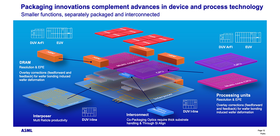
On the tool-maker front, ASML has an array of new lithography solutions, Alberto Pirati, head of portfolio management for advanced markets, said in a Tuesday presentation. One of the differences in the new technology is that it has greater stability than the old, which improves the printing of finer features, Pirati noted.
Another improvement is that the new machines have more measurement capabilities of both lithography and wafer parameters. What this advance allows is an improved ability to support processes such as those that involve bonding wafers to one another to create 3D stacks, Pirati said.
Wafers are prone to stress and warpage arising from the fabrication process, which can be an issue during bonding because the bonding process may magnify these effects. Taking measurements allows the lithography system to correct such issues by adjusting focus and making other changes.
“A lithography tool is a formidable tool to compensate process fingerprints,” Pirati said.
In another example of AI’s impact, on Wednesday Soobin Hwang, an imec researcher, presented results on his investigation into how to improve performance of extreme ultraviolet lithography (EUVL). EUVL is a key technology for patterning the most advanced chips, needed to support AI demand.
In the most common semiconductor photolithography process, light from a source interacts with a mask, and optics project the result onto a wafer coated with photoresist. After develop and etch, the result is a pattern on the wafer. In this way, fabricators build up the layers of conductors, insulators, and other elements needed to construct an integrated circuit and a functioning chip.
Hwang’s work involved sub-resolution assist features. These are small features on a mask never intended to print. Instead, they help expand the operating range of the lithography tool, thereby improving patterning and increasing yield.
“We can get a larger operating process window,” Hwang said of the imec team’s results.
Part of the reason for this improvement is that the assist features increase the depth of focus. A greater depth of focus, all other parameters being equal, makes a lithography process more robust. Hwang reported that the assist features can improve the depth of focus by as much as 29 percent in the range of chip feature sizes he studied.
However, putting assist features into a production manufacturing process will need to wait for mask variability reductions. Because they are small, the resist features experience a greater impact from these variations.
A final example of AI’s impact comes from a Monday presentation by Ting-Hung Lin, a senior manager at Nvidia. The company engineers advanced chips, systems, and software for AI. Lin is working to extend Nvidia technology and large language models to industrial applications.
Along those lines, Lin talked about work Nvidia had done in collaboration with TSMC. This work involved classifying an image map of defects found on a wafer with a system that could respond with a simple explanation of the image.
There might be, for example, a line of defects arrayed in an arc across a wafer. This could be due, Lin said, to a scratch from the arm of a piece of equipment.
Existing automated classification technology suffers from problems, Lin said. They often require thousands of images for training, and they must have those images before they can tell a normal part from an abnormal part. So, when a new type of defect appears, they do not flag it. They also must be retrained when a new product or process is introduced.
In contrast, Nvidia’s Visual Language Model requires only 50 to 100 wafer image samples or another small data set once it is past an early stage that requires a lot of data. Even during this early stage, it has the advantage of being able to do self-supervised learning, Lin said. It can also spot changes over time and identify normal versus abnormal wafer images, even when confronted with new defects.
“We have some quite promising results,” Lin said.
The models are undergoing further refinement at TSMC. The technique could also extend to other than optical imaging, with transmission electron microscopy data sets being one possibility. If the work by Nvidia is successful, AI will help manufacture the chips on which AI solutions run.
Hank Hogan is a freelance science and technology writer.
| Enjoy this article? Get similar news in your inbox |
|