Chips are headed up and down. So, lithography and related technologies will help that happen, according to presentations at the 2025 SPIE Advanced Lithography + Patterning conference.
Moore’s Law calls for a doubling of transistor counts within a packaged device every two years. For decades lithography and patterning enabled this scaling up in transistor density. Transistors got smaller in length, width, and height, allowing more of them to be packed into a given area. For most devices, this shrinkage took place on the surface of silicon wafers.
A 300-millimeter diameter wafer is 0.775 mm, which is 775 microns, thick. But the active circuitry lies at the surface, taking up a depth that is about 0.2 microns for the most advanced technology nodes. Confronted by scaling and performance problems, chip makers are now looking to move from a flat device plane into one with three dimensions.
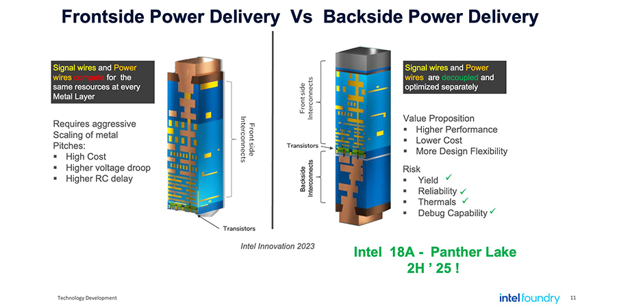
In a Tuesday presentation, Mark Phillips, director of lithography hardware and solutions at Intel, talked about backside power delivery, one of the 3D chip technologies. Intel is taking this approach because of a new 3D transistor architecture, he said.
“We couldn't get the full performance out of the new transistor without addressing the power delivery roadblock,” Phillips noted.
He added that it’s been about 25 years since there was a major change in power delivery. In contrast, new transistor architectures arrive every five to 10 years. He noted, however, that other major chip manufacturers have announced plans to implement backside power delivery.
The power bottleneck confronting chip makers is that having all signal and power lines on one side of the chip forces tradeoffs. Conducting lines that carry power should be large because that lowers resistance, benefiting power delivery. But signal lines must meet switching speed specifications and need to scale along with the rest of the circuitry when there is a shrink. These factors push signal lines to be smaller than power delivery lines. There also are congestion issues, making routing signal and power lines difficult. Hence, chip makers must compromise.
Moving the power lines to the backside of the wafer solves these problems. Power lines can be fat while signal lines can be skinnier. What’s more, they don’t run into each other, lessening congestion.
Delivering power from the back, though, brings its own challenges. For instance, wafers are thick and so for backside power delivery chip makers thin the wafers in a mechanical and chemical grinding process that takes off nearly all the silicon. One way to do this is to finish processing the front of the wafer, attach the front to a dummy wafer, then thin the back before finishing manufacturing by processing the backside. The final step is to free the now thin wafer from the dummy wafer and move on to the final processing steps.
As Phillips noted, the thinning process requires removing a lot of silicon. That removal, though, cannot damage the circuitry on the front of the wafer. Therefore, fabricators must carefully monitor and measure the material removal.
This requirement and other measurements related to 3D processing were discussed by Janusz Bogdanowicz, a principal member of the technical staff at imec who specializes in semiconductor metrology. In a Monday presentation, he noted there is now a strong emphasis on measurements related to 3D technologies, which includes backside power delivery, 3D transistors, and bonding of chips and wafers to one another.
“In the world of 3D devices, things are more complex because of this extra dimension,” he said.
To see why, consider that previously there was only a need to measure aspects of device features related to length and width because every part of the circuit was on the surface. Consequently, the important items about a measurement technique were its lateral resolution and its throughput.
Adding the third dimension means that the probing depth of a measurement method now becomes critical, Bogdanowicz pointed out. Some 3D fabrication results in long narrow holes, while other 3D manufacturing leads to films that cover objects. It may be necessary to see through die or, in the case of backside processing, peer through a wafer to determine when to stop grinding.
Bogdanowicz noted that there are many different measurement methods available today, using electrons, light, X-rays, sound, ions, or even mechanical tips. These approaches send a probe into a sample and then collect information about how the sample reacts, using this data to extract data about important parameters. The measurement methods vary in how small an object they can measure, with some in the nanometer range and others in the 100-micron regime. Some of the methods have a probing depth greater than a full wafer while others can only penetrate a single transistor.
Bogdanowicz noted that in the 2D world, probing depth was not important. When engaged in 3D semiconductor manufacturing, having enough probing depth is a critical requirement, he stated.
So, the addition of a third dimension to semiconductor manufacturing significantly changes measurements needed and alters their evaluation, Bogdanowicz said. “It completely changes how we should look at things.”
Hank Hogan is a freelance science and technology writer.
| Enjoy this article? Get similar news in your inbox |
|