Unlike what happens in Las Vegas, what happens in a wafer fab doesn’t stay there. That’s why the use of PFAS (Per- and Polyfluoroalkyl Substances) materials in semiconductor manufacturing is a concern. In lithography, PFAS plays crucial roles in the patterning of photoresist, and they present long term health and environmental hazards.
“Once released, PFAS can exist for long periods without breaking down,” said Yuzuru Kaneko, leader of the photoresist material development team for Central Glass Co. “It is important to support their reduction.”
Two presentations on Wednesday during the 2025 SPIE Advanced Lithography + Patterning conference highlighted progress in this area. In the first presentation, Kaneko spoke about eliminating PFAS in 193-nm immersion lithography, a widely used semiconductor patterning approach.
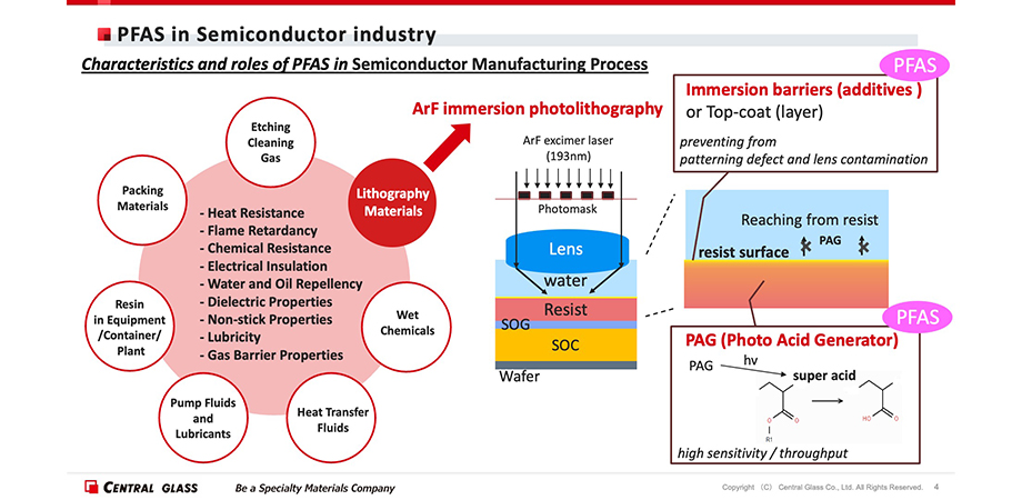
Central Glass has designed a PFAS-free photo acid generator and a PFAS-free immersion barrier polymer. These two substances are in patterning a wafer.
In immersion lithography, fabricators coat the wafer with photoresist and top it with an immersion barrier. Immersion lithography involves squirting water onto the wafer, with this water forming the last element in the optical chain that projects the mask image onto the wafer.
This top coating keeps the water from interacting with the resist and disrupting the exposure process. As for the acid generator, 193-nm resists are chemically amplified. A single photon striking the resist is magnified by a chemical reaction so that eventually what can be hundreds or thousands of resist molecules link together. This amplification starts when the photon interacts with an ultraviolet sensitive photoacid generator.
Of course, any new PFAS-free formulations of photoresist components must work as well as the existing ones, which contain PFAS. So, as part of its development efforts, Central Glass evaluated its new PFAS-free substances for a host of parameters. To take one example, company researchers looked at the transmissibility of the immersion barrier at 193-nm, a crucial parameter because the barrier is supposed to keep water out but let exposure light through. Tests showed the transmittance to be 95 percent, a high figure.
Once they were sure the new materials met requirements, the researchers then patterned wafers. These tests indicated that the PFAS-free materials performed well. The new materials are now in production, and Kaneko said that development work on further enhancement continues.
In her Wednesday presentation, Ionela-Daniela Carja, a researcher with Merck Electronics KGaA, began by noting that PFAS landscape is complex, with different definitions offered by different organizations. There is a chance, she noted, that regulations will expand to include any fluorine containing compound.
For that reason, the company’s goal is to have products be more than PFAS-free. “We are really going forward to offer a comprehensive fluorine-free solution,” Carja said.
To do this, researchers modeled proposed molecules to predict reaction strengths. They then selected the most promising to synthesize for further assessment.
One of the areas the team investigated was top anti-reflective coating or TARC. As the name suggests, these substances go on top of the resist and reduce reflections. Without them, printed features are bigger or smaller than the ideal, with this difference varying by resist thickness. Tests indicated that the fluorine-free, top anti-reflective coating did better at controlling this swing than its fluorinated counterpart. The researchers confirmed this superiority by printing a series of lines and spaces, followed by measuring the resulting toothed array.
“Our fluorine-free TARC material can generate nice uniformity,” Carja said.
She noted that the group had also developed photoresists and other components needed for fluorine-free lithography. These include both positive tone resists, where the resist pattern on the wafer looks like what is on the mask, as well as negative tone resists, where the pattern on the wafer is the inverse of what is on the mask.
During a Q&A after her talk, Carja said that the immediate goal is to produce materials that match current resists. However, switching platforms from old to new material also offers an opportunity, one that the team hopes to exploit by working to achieve even further improvements.
“We want to take advantage of this platform and push it to the final limits,” Carja said.
Hank Hogan is a freelance science and technology writer.
| Enjoy this article? Get similar news in your inbox |
|