Meeting semiconductor challenges with lithography
At Monday talks that opened SPIE’s 2025 Advanced Lithography + Patterning conference, two speakers outlined challenges facing the semiconductor industry, like the need for greater energy efficiency or heat management. They also discussed potential solutions, including changes in transistor layout and materials. Success in dealing with the issues confronting the industry, they noted, could pave the way for transformative technologies, like humanoid robots.
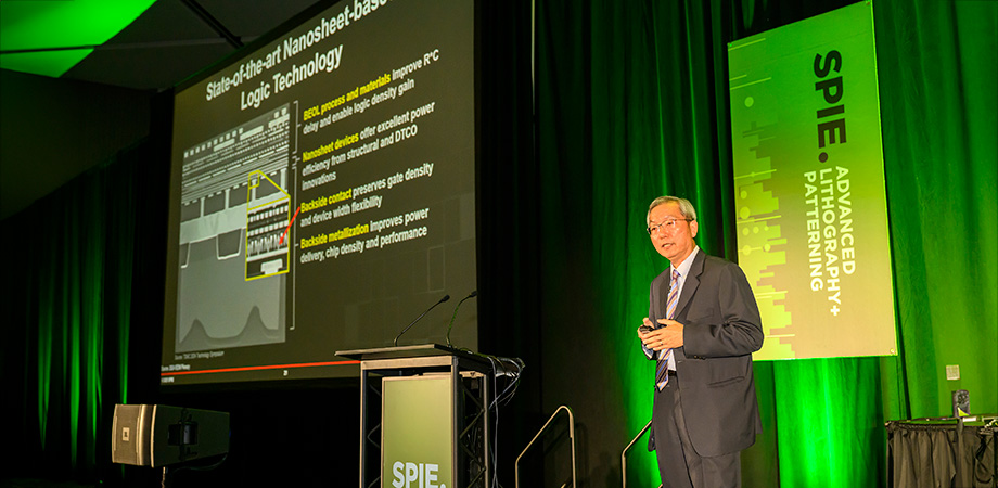
In the first of the two presentations, Shien-Yang Wu, vice president of advanced technology development at TSMC, noted the rapid evolution of generative AI. This technology, found in ChatGPT and other large language models, is driving the expansion of data centers. One consequence is exponential growth in energy demands, with data centers seeing a 12-fold increase in power needs per year. That, in turn, forces change on the underlying semiconductor technology.
“Energy efficient compute is absolutely required,” Wu said.
To address this need, the industry is implementing new technologies. TSMC and others are changing transistor architecture. Traditionally, transistors have been flat, with individual components sitting alongside each other. TSMC is implementing a layout in which parts of the transistor sit atop one another. Such an arrangement increases transistor density 1.5 to 2.0 times, while improving performance.
Discussing another approach being taken to address performance and density issues, Wu reported that chip design and process technology co-optimization have led to a 130 X improvement in energy efficiency over the last seven process nodes. Those co-optimizations also increased how many integrated circuit elements can be packed into each chip. Extending co-optimization to the system those chips go into, something TSMC is now doing, will further improve performance, Wu predicted.
In the future, there could be new materials, with one possibility being carbon nanotubes. These rolled up sheets of carbon atoms are only a nanometer in diameter and offer high carrier mobility, helpful when making fast devices.
Wu also mentioned ways in which the AI made possible by semiconductors is making it easier to make semiconductors. For example, extreme ultraviolet lithography, or EUVL, uses 13.5 nm wavelength photons produced by hitting a droplet of tin 50,000 times a second with an infrared laser pulse. The resulting plasma radiates EUV photons – and can also lead to tin ending up on nearby optics. That contamination degrades optical efficiency and leads to wasted power. Using AI machine learning, engineers were able to tune the pulse, improve the plasma formation, decrease the amount of tin contamination, and reduce energy consumption, Wu said.
At the end of his talk, he noted a synergy between AI and semiconductors. Future advances, though, require collaboration.
“Let’s work together and make it happen,” Wu said.
In the next plenary talk, Subramanian S. Iyer, a professor who heads UCLA’s Center for Heterogeneous Integration and Performance Scaling, discussed strategic directions for electronics packaging. He noted that packaging has traditionally focused on a single die, emphasizing protection of the chip against environmental and mechanical threats.
Advanced packaging, on the other hand, seeks to deliver power and get rid of heat. The power to switch each transistor is less for the latest technology nodes as compared to the power needed for earlier nodes. But the latest nodes also allow chip makers to put more transistors on a chip and in a package, which means that there is more heat. That thermal burden is only going to grow as the march of semiconductor technology continues.
“Getting that heat out is going to be very difficult,” Iyer said about future chips.
Advanced packaging also seeks to have better electrical connections between chips. In the past, chip designers kept making chips bigger and bigger because moving data around on a die was so much more efficient than moving it on to and off a chip. But the result has been that chips are as large as they can get, bumping up against the maximum size allowed by lithography tools. In response, designers are now turning to a main chip and chiplets, each one of these a smaller die that performs specialized functions.
To maintain performance of the overall assembly of chips and chiplets these different pieces of silicon must be packaged together. What’s more, they need to be electrically connected in a way that makes data movement easy. This requires numerous short connections between chips and chiplets, Iyer said.
He added that industrial and academic researchers are working on this problem. Some of the possible solutions borrow from the techniques used to pattern silicon today, and Iyer thinks that such technology could be a critical piece of the answer.
“Lithography in some form is a very important part,” he said.
| Enjoy this article? Get similar news in your inbox |
|