Extreme ultraviolet lithography, or EUVL, is a hot topic at the 2025 SPIE Advanced Lithography + Patterning conference. EUVL technology continues to evolve, as evidenced by presentations on the progress of its numerical aperture (NA). Today’s EUVL tools have an NA of 0.33. Upcoming semiconductor technology nodes, though, will push those systems to their resolution limit and beyond. So, the industry is racing to deploy 0.55 high NA tools. On the drawing boards there are 0.75 hyper NA tools.
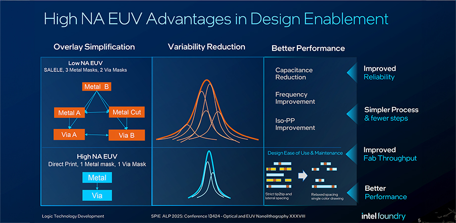
“High NA avoids excessive multipatterning,” said Steven Carson, the lead technologist for Intel Foundry’s high NA tool, in explaining this move up in NA during a Mondary afternoon talk. He noted that processing with high-NA EUV can cut manufacturing steps fourfold for upcoming technology nodes as compared to the current 0.33 NA EUV.
In determining the minimum feature size that a lithography tool can print, one variable is wavelength of the light. In the case of EUVL, that is 13.5 nanometers, 14 times smaller than that available with a 193-nm deep UV photolithography system. So, an EUV system can print something 14 times smaller than a deep UV tool, all things being equal.
But there’s another resolution impacting factor to consider: NA. A higher NA makes it possible to resolve smaller features. So, if technologists crank up the NA of a lithography tool, it can pattern smaller features.
An alternative is to do double patterning. In this approach one pass through the process patterns half of the total image. A subsequent pass creates the rest. The technique works and chip makers used it to extend the capabilities of deep UV lithography, a requirement because the EUVL implementation was slow to arrive.
The double patterning approach, though, involves more process steps and adds another wrinkle: overlay. The second pass must be precisely aligned to the first or else there will be a break in lines, the touching of lines that should be separate, or another defect.
Going with high-NA EUV avoids having to do double patterning. In an example cited by Carson, high-NA patterning requires two layers instead of five needed for double patterning using 0.33 NA tools.
“You greatly simplify your overlay scheme,” he said.
High-NA EUV also brings benefits in terms of reduced variability because of the need to control fewer layers. That simplification minimizes the variation in feature size and quality from spot to spot across a wafer.
There is, though, a price to pay in moving up in numerical aperture. A higher NA leads to a shallower depth of focus. Thus, focal control must be tighter. There also is a smaller field of view, which impacts the masks used.
Still, the semiconductor industry hopes to deploy high-NA technology sooner rather than later. Carson noted that it took over seven years from the availability of 0.33 NA tools to their use in manufacturing. A similar wait for high-NA tools means double patterning would again be needed.
Intel, therefore, worked with tool supplier ASML and research consortium imec to minimize the deployment time of high-NA EUV and avoid this problem. The standard practice is to completely assemble a novel lithography tool at the factory, test it, and certify it. The supplier then disassembles the tool and ships it to the user. The end user then puts the tool back together, tests it, and certifies it.
For the high-NA EUV rollout, Intel and its suppliers chose to qualify the modules, with the final total assembly done at Intel’s facility. “We saved months in cycle time,” Carson said.
Intel also opted to do other tasks in parallel. Thus, it selected a photoresist and worked on aspects of mask making before the tool was ready. Testing and validation of the tool and process are still under way, but Carson reported that results so far look good.
| Enjoy this article? Get similar news in your inbox |
|